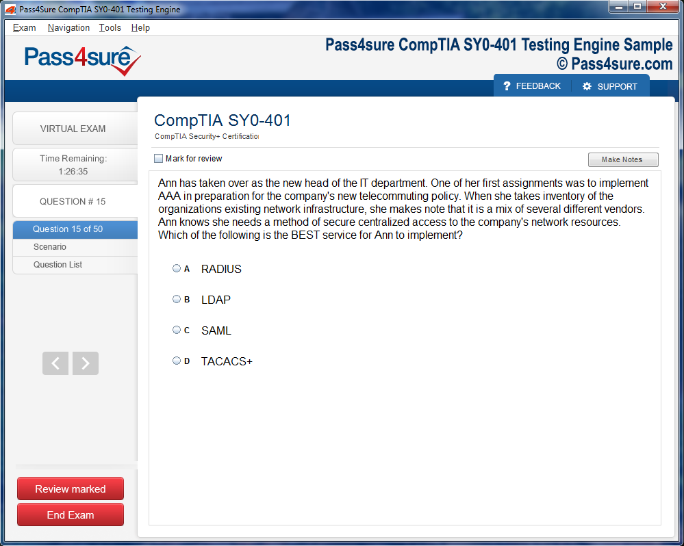
Product Screenshots


Frequently Asked Questions
How does your testing engine works?
Once download and installed on your PC, you can practise test questions, review your questions & answers using two different options 'practice exam' and 'virtual exam'. Virtual Exam - test yourself with exam questions with a time limit, as if you are taking exams in the Prometric or VUE testing centre. Practice exam - review exam questions one by one, see correct answers and explanations.
How can I get the products after purchase?
All products are available for download immediately from your Member's Area. Once you have made the payment, you will be transferred to Member's Area where you can login and download the products you have purchased to your computer.
How long can I use my product? Will it be valid forever?
Pass4sure products have a validity of 90 days from the date of purchase. This means that any updates to the products, including but not limited to new questions, or updates and changes by our editing team, will be automatically downloaded on to computer to make sure that you get latest exam prep materials during those 90 days.
Can I renew my product if when it's expired?
Yes, when the 90 days of your product validity are over, you have the option of renewing your expired products with a 30% discount. This can be done in your Member's Area.
Please note that you will not be able to use the product after it has expired if you don't renew it.
How often are the questions updated?
We always try to provide the latest pool of questions, Updates in the questions depend on the changes in actual pool of questions by different vendors. As soon as we know about the change in the exam question pool we try our best to update the products as fast as possible.
How many computers I can download Pass4sure software on?
You can download the Pass4sure products on the maximum number of 2 (two) computers or devices. If you need to use the software on more than two machines, you can purchase this option separately. Please email sales@pass4sure.com if you need to use more than 5 (five) computers.
What are the system requirements?
Minimum System Requirements:
- Windows XP or newer operating system
- Java Version 8 or newer
- 1+ GHz processor
- 1 GB Ram
- 50 MB available hard disk typically (products may vary)
What operating systems are supported by your Testing Engine software?
Our testing engine is supported by Windows. Andriod and IOS software is currently under development.
Mastering Serial Peripheral Interface (SPI): Everything You Need to Know
The Serial Peripheral Interface (SPI) emerges as a quintessential conduit for synchronous data exchange, weaving an intricate lattice of communication between microcontrollers and peripheral entities. Operating within a master-slave hierarchy, SPI delineates distinct channels for clock signaling (SCK) and bidirectional data transfer, with MISO serving as the pathway from slave to master, and MOSI channeling information from master to slave. The inclusion of a slave select (SS) line orchestrates the engagement of multiple peripheral devices, enabling meticulous device addressing. This architecture facilitates full-duplex communication, permitting the simultaneous transmission and reception of information, thus optimizing temporal efficiency and signal fidelity.
The Serial Peripheral Interface, commonly known as SPI, is a cornerstone in the realm of embedded systems and digital electronics, enabling seamless communication between microcontrollers, memory devices, sensors, and a myriad of peripherals. SPI distinguishes itself by being a synchronous serial communication protocol, which means data transfer is coordinated by a shared clock signal, ensuring precise timing and predictable communication. Unlike asynchronous protocols such as UART, SPI relies on this clock line to synchronize data exchange, allowing for faster and more reliable transfers across short distances in embedded systems.
At its core, SPI operates on a master-slave paradigm. The master device generates the clock signal and initiates communication, while the slave devices respond based on the master’s commands. Typically, SPI utilizes four fundamental signals: SCLK (serial clock), MOSI (Master Out Slave In), MISO (Master In Slave Out), and CS (chip select). SCLK orchestrates the timing of data transfer, while MOSI and MISO facilitate bidirectional communication. The CS line allows the master to selectively activate a specific slave device, ensuring that multiple peripherals can coexist on the same bus without interference. This simplicity and predictability make SPI an ideal protocol for high-speed applications where deterministic timing is crucial.
One of the defining advantages of SPI is its exceptional data transfer rate. Unlike I²C, which relies on addressing schemes and can be limited by bus arbitration, SPI can achieve multi-megahertz throughput, making it suitable for applications demanding high-speed memory access, sensor data streaming, or real-time control. This is particularly important in scenarios like audio processing, graphical displays, and data acquisition systems, where even microsecond delays can impact performance. Moreover, SPI supports full-duplex communication, allowing data to be transmitted and received simultaneously, further enhancing efficiency in complex embedded systems.
SPI’s flexibility extends beyond speed and simplicity. Variants such as QSPI (Quad SPI) and Octal SPI have emerged to meet the growing demand for higher bandwidth. QSPI leverages four data lines instead of one, effectively quadrupling the data transfer rate, while Octal SPI uses eight lines for even greater throughput. These high-performance interfaces are particularly beneficial for interfacing with PSRAM and NOR Flash memory, where fast read and write cycles are critical. XSPI, another evolution, introduces additional clocking flexibility and enhanced control, making it ideal for sophisticated applications requiring both speed and versatility.
Despite its many advantages, SPI comes with certain trade-offs. It requires more wiring than protocols like I²C, which can complicate PCB design, especially in space-constrained applications. Additionally, SPI does not inherently include error checking or collision detection, so designers often need to implement supplementary mechanisms to ensure data integrity in noisy environments. Furthermore, while SPI excels in short-distance communication, its performance can degrade over longer lines due to signal reflections and electromagnetic interference, necessitating careful layout and possibly signal conditioning for robust operation.
In practical applications, SPI has become ubiquitous. It underpins memory interfacing, sensor networks, display modules, and communication between microcontrollers and peripherals in industrial, automotive, and consumer electronics systems. Its combination of high speed, low latency, and deterministic timing makes it indispensable in real-time systems where performance and reliability cannot be compromised. By mastering SPI and its advanced variants, engineers can unlock efficient data exchange, streamline embedded design, and enhance the overall responsiveness and capability of their systems.
Ultimately, understanding SPI is not merely about memorizing pin configurations or transfer modes; it is about appreciating the underlying principles that govern synchronous communication, the trade-offs involved, and the innovations that continue to push its performance boundaries. SPI remains a vital skill in the engineer’s toolkit, bridging the gap between processing power and peripheral capabilities, and enabling the creation of sophisticated, high-performance embedded systems.
SPI’s structural elegance lies in its minimalist yet potent design. The interplay of clock polarity (CPOL) and clock phase (CPHA) governs the cadence of data transfer, dictating precise temporal alignment between sender and receiver. Typically configured in a four-wire schema encompassing SCK, MOSI, MISO, and SS, SPI endows the master with comprehensive control over data flow and clock generation, while ensuring robust isolation and synchronization among connected slaves. This structural paradigm reduces latency and bolsters signal integrity across diverse operational environments.
The ubiquity of SPI in embedded systems stems from its dexterous adaptability. Peripheral devices such as sensors, digital displays, non-volatile memory modules, and specialized interface chips exploit SPI’s simplicity and rapid throughput. Its cost-effectiveness, coupled with facile implementation, renders it particularly attractive for scenarios demanding moderate data rates without the intricacies of more complex communication protocols. From industrial monitoring systems to consumer electronics, SPI’s presence is pervasive, underlining its role as a foundational pillar in contemporary digital communication.
Evolution of SPI Architectures
SPI’s lineage can be traced to rudimentary synchronous serial communications, yet its modern iterations exhibit nuanced enhancements in operational versatility. Early implementations prioritized basic signal exchange, yet contemporary variants integrate features such as enhanced clock management, multi-slave orchestration, and error detection mechanisms. These augmentations broaden SPI’s applicability, extending its utility beyond conventional embedded systems into domains requiring stringent timing and reliability constraints.
The evolution of SPI architectures also reflects the exigencies of high-speed and energy-efficient designs. By modulating clock frequencies and optimizing signal integrity, modern SPI configurations facilitate rapid data acquisition from high-resolution sensors or memory modules. Moreover, the expansion of SPI into multi-master configurations permits collaborative data exchanges between multiple control units, mitigating bottlenecks in complex electronic ecosystems.
Advantages and Limitations
SPI’s allure is anchored in its straightforward implementation and high throughput potential. Unlike asynchronous protocols, SPI ensures deterministic timing, which is paramount for real-time applications. The full-duplex nature of communication allows concurrent read and write operations, thereby enhancing efficiency. Additionally, the protocol’s scalability accommodates multiple peripheral devices, provided that distinct slave select lines are available, which simplifies integration within multi-component systems.
Nonetheless, SPI is not without constraints. Its reliance on dedicated lines for each slave device can impose hardware overhead in dense systems. The absence of intrinsic error correction necessitates auxiliary mechanisms for data integrity assurance. Furthermore, the protocol’s short-distance orientation limits its efficacy in extensive networks, necessitating additional considerations for signal attenuation and electromagnetic interference.
SPI in Modern Embedded Systems
Within contemporary embedded systems, SPI maintains a prominent position due to its balance of simplicity and performance. High-fidelity sensors, touchscreens, and flash memory components frequently interface via SPI, benefiting from the protocol’s low latency and deterministic timing. Embedded developers leverage SPI to orchestrate rapid data acquisition and responsive control loops, ensuring that real-time constraints are met without excessive computational burden.
The adaptability of SPI extends to its coexistence with other communication protocols. Hybrid architectures often deploy SPI alongside I²C or UART, allowing developers to capitalize on SPI’s speed while exploiting the low-pin-count or long-distance advantages of alternative protocols. This hybridization amplifies system versatility, catering to diverse operational requirements while maintaining coherent data orchestration.
Technical Nuances and Optimization Strategies
Optimizing SPI communication entails careful calibration of clock polarity, phase alignment, and signal timing. Variations in CPOL and CPHA settings influence sampling instances, impacting data integrity and transmission efficiency. By meticulously aligning these parameters with peripheral requirements, developers can maximize throughput while minimizing errors.
Signal integrity strategies, including impedance matching and termination resistors, further enhance SPI reliability, particularly in high-frequency implementations. Additionally, software-level optimizations such as buffering, direct memory access (DMA), and interrupt-driven data handling reduce processor overhead and elevate system responsiveness. These techniques collectively cultivate a communication ecosystem that balances speed, precision, and robustness.
SPI in Sensor Networks
The deployment of SPI in sensor networks underscores its utility in rapid data acquisition. Environmental sensors, motion detectors, and biometric devices often necessitate prompt and precise data retrieval, a requirement that SPI fulfills with aplomb. By ensuring synchronized clocking and minimizing latency, SPI facilitates real-time monitoring and control, empowering applications ranging from industrial automation to consumer wearables.
Moreover, SPI’s deterministic timing enables sophisticated data fusion techniques, wherein multiple sensor readings are aggregated and processed with temporal coherence. This capability is crucial in scenarios demanding high-resolution measurements or predictive analytics, allowing embedded systems to react intelligently to dynamic conditions.
Memory Interface Applications
SPI’s role in memory interfacing is particularly pronounced, given the proliferation of non-volatile storage solutions. Flash memory, EEPROMs, and other serial memory devices exploit SPI’s high-speed, low-latency communication to deliver rapid read and write cycles. The protocol’s deterministic control over clock and data lines ensures data integrity, particularly during sequential operations or burst transfers.
Advanced memory controllers often leverage SPI in conjunction with error-detecting codes and write-protection mechanisms, augmenting reliability in mission-critical applications. From firmware storage in embedded devices to archival data repositories, SPI remains a cornerstone of modern memory interfacing strategies.
SPI in Display Modules
Visual interfaces, ranging from simple alphanumeric screens to complex graphical displays, frequently utilize SPI for data exchange. The protocol’s rapid throughput enables high refresh rates and fluid visual rendering, while its simplicity allows for straightforward integration with microcontroller-driven graphics pipelines.
By leveraging SPI, display modules can achieve precise timing control, ensuring that pixel data is synchronized with frame updates. This capability is instrumental in applications demanding dynamic visualization, such as wearable devices, control panels, and interactive kiosks. The minimal hardware overhead further accentuates SPI’s appeal in compact or power-constrained designs.
Future Prospects of SPI
As digital ecosystems evolve, SPI continues to adapt, embracing higher frequencies, lower power consumption, and augmented error management features. Emerging applications, including Internet of Things (IoT) nodes, autonomous vehicles, and advanced robotics, increasingly rely on SPI for swift, reliable data exchange.
Innovations in multi-master and daisy-chain configurations promise to enhance scalability, permitting complex networks of devices to communicate efficiently without excessive wiring. Additionally, ongoing research into low-voltage, high-speed signaling aims to expand SPI’s applicability in ultra-compact or energy-sensitive devices, ensuring its relevance in the next generation of embedded technology.
The Serial Peripheral Interface stands as a paragon of simplicity, reliability, and adaptability within the realm of embedded systems. Its master-slave architecture, full-duplex capabilities, and deterministic timing render it indispensable for a multitude of peripheral interactions. While not devoid of limitations, SPI’s enduring utility is affirmed through its pervasive presence in sensor networks, memory interfaces, display modules, and broader embedded ecosystems. As technological frontiers advance, SPI’s evolution continues to meet the demands of high-speed, high-integrity communication, cementing its status as a foundational protocol in contemporary digital design.
Understanding the Essence of XSPI
The Extended Serial Peripheral Interface, colloquially abbreviated as XSPI, represents an evolutionary leap from the conventional SPI protocol, transcending traditional limitations while preserving seamless backward compatibility with antecedent SPI devices. XSPI emerges as an architectural paradigm engineered for applications necessitating elevated data transfer velocities without compromising the integrity of historical peripheral ecosystems. Unlike the rudimentary SPI standard, XSPI orchestrates a symphony of data lines and clock frequencies, coalescing into a framework that optimizes both speed and scalability. This technological augmentation offers engineers the capacity to interweave legacy devices with next-generation high-throughput peripherals, thereby mitigating obsolescence and fostering longevity in electronic systems.
Technical Enhancements and Architectural Innovations
XSPI is not merely an incremental improvement; it embodies a comprehensive recalibration of serial communication architecture. The protocol extends support to supraharmonic clock frequencies, a feature that dramatically amplifies data throughput relative to its SPI predecessor. By facilitating multiple transmission modalities—including Single, Dual, Quad, and Octal data lanes—XSPI accommodates diverse bandwidth requisites with precision. The duality of compatibility and performance enables intricate data pipelines, permitting concurrent read and write operations while minimizing latency. Additionally, the protocol incorporates sophisticated signal integrity mechanisms, including skew compensation and dynamic drive-strength adjustments, which are pivotal in maintaining high-fidelity communication across extended traces and complex PCB layouts. This meticulous engineering ensures XSPI can thrive in environments where conventional SPI would succumb to bottlenecks.
Multi-Lane Data Transmission and Scalability
The quintessence of XSPI lies in its adeptness at multi-lane transmission. Traditional SPI, confined to a single data line, often encounters throughput constraints in high-speed applications. XSPI counters this limitation by leveraging Dual, Quad, and Octal modes, thereby multiplying effective bandwidth without necessitating fundamental alterations to device architecture. Such scalability is not merely theoretical; it manifests in real-world applications where the need for simultaneous data streams is paramount. For instance, in high-resolution imaging or real-time data acquisition systems, XSPI’s multi-lane capabilities enable rapid buffer transfers, enhancing system responsiveness and reducing perceptible latency. The protocol’s architecture, therefore, is not a mere iteration but a holistic redesign aimed at amplifying throughput while retaining modular adaptability.
Compatibility with Legacy SPI Devices
One of XSPI’s most salient attributes is its unwavering commitment to backward compatibility. Despite its advanced capabilities, XSPI maintains operational coherence with legacy SPI peripherals, allowing for hybrid systems where next-generation and historical devices coexist harmoniously. This ensures that system designers can leverage high-speed capabilities without the prohibitive costs or logistical challenges associated with wholesale hardware replacement. The protocol’s intelligence in negotiating device modes—automatically adjusting lane configurations and clock frequencies based on peripheral capabilities—renders it remarkably versatile. Consequently, XSPI embodies a bridge between temporal technological layers, facilitating continuity while propelling system performance into contemporary echelons.
Enhanced Data Integrity and Reliability
High-speed data transmission invariably introduces susceptibility to errors, jitter, and signal degradation. XSPI addresses these challenges with a repertoire of reliability-enhancing features. Adaptive timing calibration dynamically aligns data lines to mitigate skew and crosstalk, while error-checking routines embedded within the protocol safeguard against corruption during high-frequency operation. Furthermore, XSPI accommodates robust electrical signaling schemes, allowing it to operate across variable voltage domains and diverse environmental conditions. Such resilience ensures that critical applications, including autonomous systems, medical instrumentation, and industrial automation, can rely on XSPI for consistent, high-fidelity communication under demanding circumstances.
Applications in High-Resolution Displays
In contemporary electronics, high-resolution display systems necessitate voluminous data transfers at rapid intervals. XSPI emerges as a quintessential interface for these applications, providing the bandwidth required to drive ultra-high-definition screens and touch-sensitive panels. Its multi-lane capability facilitates parallel data pipelines, enabling swift refresh rates and minimizing perceptible lag. Moreover, XSPI’s backward compatibility allows integration with existing display controllers, ensuring that the evolution to higher-speed protocols does not necessitate a complete redesign. This amalgamation of performance and adaptability positions XSPI as a linchpin in the proliferation of visually immersive, responsive display technologies.
Optimizing Flash Memory Performance
Flash memory systems, particularly those leveraging NOR or NAND architectures, benefit profoundly from XSPI’s enhanced data throughput. Traditional SPI interfaces often impose latency constraints during read and write cycles, impeding the overall system performance. XSPI, with its scalable lane configuration, circumvents these bottlenecks, enabling rapid memory access and expeditious boot sequences. The protocol’s architecture allows concurrent execution of multiple memory transactions, optimizing both random and sequential access patterns. This is particularly consequential in high-performance computing environments, embedded systems, and consumer electronics, where instantaneous memory responsiveness directly correlates to user experience and operational efficiency.
High-Performance Sensors and Real-Time Data Acquisition
In domains such as robotics, aerospace, and industrial automation, sensors produce continuous streams of data requiring rapid, reliable transmission. XSPI’s high-speed interface is ideally suited for real-time data acquisition, allowing multiple sensor arrays to feed information simultaneously without overwhelming system bandwidth. The protocol’s low-latency characteristics ensure that data propagation occurs almost instantaneously, supporting applications where temporal precision is critical. Moreover, XSPI’s error-mitigation strategies guarantee that sensor readings remain accurate even under electrically noisy conditions, bolstering both reliability and safety in mission-critical scenarios.
Integration in Embedded Systems
Embedded systems, characterized by compact form factors and stringent power budgets, often confront limitations imposed by traditional communication protocols. XSPI’s efficiency-oriented design addresses these challenges by facilitating high-speed data transfers without incurring significant power overhead. Its modular architecture allows selective activation of multiple data lanes, balancing speed requirements with energy conservation. Furthermore, the protocol’s compatibility with legacy SPI devices ensures that embedded platforms can integrate advanced peripherals without necessitating extensive redesigns. This adaptability renders XSPI a highly versatile choice for microcontroller-centric systems, Internet of Things (IoT) devices, and compact industrial controllers.
Industrial Automation and Robotics
In industrial automation, real-time control and rapid data exchange are indispensable. XSPI’s high-throughput capabilities enable robotic systems and automation controllers to coordinate complex operations with minimal latency. Multi-lane data transmission allows simultaneous command dissemination and status monitoring, enhancing operational efficiency. Additionally, XSPI’s reliability mechanisms ensure that communication remains uncorrupted amidst electrical interference common in industrial environments. Consequently, the protocol not only elevates performance but also contributes to the robustness and predictability of automated systems, which are critical metrics in manufacturing and process control sectors.
Aerospace and Defense Applications
Aerospace and defense technologies often operate under stringent performance, reliability, and environmental standards. XSPI’s architecture, which accommodates high clock frequencies and multi-lane data modalities, aligns perfectly with these rigorous requirements. Avionic systems, unmanned vehicles, and tactical instrumentation benefit from the protocol’s ability to maintain high-speed, error-resilient communication across long distances and in electrically noisy environments. Moreover, XSPI’s backward compatibility allows integration with pre-existing SPI-based subsystems, ensuring continuity in mission-critical applications while simultaneously enhancing overall data throughput and responsiveness.
Data-Centric Internet of Things (IoT) Devices
The proliferation of IoT devices has generated an unprecedented demand for high-speed, low-latency communication interfaces. XSPI, with its capability to transmit substantial amounts of data rapidly across multiple lanes, is ideally suited for connected sensors, gateways, and edge devices. Its adaptive configuration allows IoT systems to optimize performance dynamically, toggling between Single, Dual, Quad, or Octal modes based on instantaneous bandwidth requirements. This adaptability not only enhances device responsiveness but also conserves energy, a critical consideration for battery-powered or energy-harvesting IoT deployments.
System Design Considerations and Implementation Strategies
Implementing XSPI in a complex system requires careful consideration of electrical and timing parameters. PCB trace lengths, signal integrity, and termination resistances must be meticulously calibrated to fully exploit the protocol’s high-frequency capabilities. Moreover, device initialization sequences and lane negotiation protocols must be precisely orchestrated to ensure optimal performance. Engineers often employ simulation and modeling tools to predict system behavior, thereby minimizing trial-and-error adjustments during physical implementation. Such rigor in design ensures that XSPI delivers both maximal throughput and long-term reliability in diverse electronic ecosystems.
Future Prospects and Evolutionary Trajectories
The trajectory of XSPI suggests continued innovation in high-speed serial communication protocols. As data-intensive applications proliferate—ranging from augmented reality to autonomous systems—the demand for protocols capable of maintaining elevated throughput without sacrificing reliability will intensify. Future enhancements may include adaptive lane reconfiguration, enhanced error correction algorithms, and tighter integration with system-level memory architectures. These prospective innovations will solidify XSPI’s role as a cornerstone of next-generation electronics, bridging the gap between legacy devices and emerging high-performance peripherals with elegance and efficiency.
Comparative Advantage Over Traditional SPI
While traditional SPI remains a reliable choice for low-to-moderate data rate applications, XSPI indisputably surpasses it in performance, scalability, and adaptability. The protocol’s support for multiple data lanes, higher clock frequencies, and sophisticated error-mitigation mechanisms provides a substantive advantage in high-demand scenarios. Furthermore, XSPI’s backward compatibility ensures that system upgrades do not necessitate wholesale replacement of existing peripherals, a factor that significantly reduces costs and complexity. In essence, XSPI combines the virtues of tradition with the imperatives of contemporary performance, achieving a balance rarely seen in serial communication protocols.
XSPI represents an elegant confluence of speed, scalability, and compatibility. Its advanced architectural features, including multi-lane transmission, adaptive error correction, and backward compatibility, render it a versatile interface suitable for a wide spectrum of applications—from high-resolution displays and flash memory to embedded systems, industrial automation, and IoT networks. By transcending the constraints of traditional SPI, XSPI enables engineers to craft electronic systems that are both forward-looking and harmoniously integrated with existing hardware. In the ever-evolving landscape of high-speed communication, XSPI stands as a testament to thoughtful innovation, bridging past and future with precision, reliability, and ingenuity.
Understanding the Quad Serial Peripheral Interface (QSPI)
The Quad Serial Peripheral Interface, abbreviated as QSPI, manifests as a sophisticated evolution of the conventional SPI protocol, designed to transcend conventional limitations in data transmission velocity. Unlike its predecessor, QSPI leverages a quartet of data lines, DQ0 through DQ3, facilitating simultaneous multibit transfer that exponentially augments throughput. This parallelization is central to its ability to sustain elevated clock frequencies while mitigating the latency endemic to traditional serial protocols. The integration of Double Data Rate (DDR) mechanisms further amplifies temporal efficiency, enabling data transfer on both the rising and falling edges of the clock signal, thereby optimizing channel utilization and rendering QSPI indispensable in high-demand environments.
QSPI’s architecture, while superficially reminiscent of SPI, incorporates nuanced refinements that substantively impact operational efficacy. The four-line configuration permits concurrent transmission of four bits per clock cycle, a stark contrast to the unilinear data path of SPI. This inherently multiplies data density, reducing the temporal overhead associated with sequential bit transfer. Additionally, QSPI accommodates both single and dual flash memory addressing schemes, enhancing its adaptability across varied hardware ecosystems. These technical augmentations collectively yield a conduit capable of sustaining elevated data throughput while maintaining electrical and timing integrity—a critical attribute in precision-dependent applications.
Technical Features
The quintessential technical hallmark of QSPI lies in its multidimensional data conduits. The quartet of parallel lines, DQ0 through DQ3, constitutes the core vector through which information traverses, ensuring that multiple bits per cycle are concurrently communicated. This is augmented by the employment of DDR protocols, which, by harnessing both clock edges, effectively double the effective data rate without necessitating additional frequency scaling. Such temporal efficiency is crucial in systems where microsecond-scale latency reduction can directly influence overall performance.
QSPI’s clocking capabilities are equally noteworthy. Where conventional SPI may falter at elevated frequencies due to signal integrity degradation or propagation delay, QSPI’s refined design ensures minimal skew and robust timing margins. The interface also provides for various operational modes, including single, dual, and quad I/O configurations, each modulating the trade-off between pin usage and transfer speed. Moreover, it often supports command sequences that allow for advanced operations such as page programming, sector erasure, and memory-mapped access, rendering it versatile for both storage and streaming applications.
From an electrical perspective, QSPI is engineered to balance speed with resilience. The differential capacitance along parallel lines is carefully managed to preclude crosstalk, while impedance matching techniques reduce signal reflection. Collectively, these features endow QSPI with the capacity to reliably deliver high-bandwidth communication even in electromagnetically noisy or densely packed circuit environments, making it a preferred interface for contemporary embedded systems.
Applications
QSPI finds its preeminence in scenarios demanding rapid data transfer, low latency, and high operational fidelity. One prominent domain is non-volatile flash memory, where the ability to read and write data at quad-line speeds dramatically enhances system responsiveness. Memory-mapped QSPI configurations allow microcontrollers and processors to treat external flash memory as an extension of internal RAM, thereby streamlining code execution and reducing access delays.
In networking and communications, QSPI serves as a conduit for Ethernet controllers, Wi-Fi modules, and other high-throughput transceivers, where millisecond-level lag can compromise system efficacy. Its rapid transactional capability enables real-time data acquisition, signal processing, and buffering, facilitating applications ranging from industrial automation to high-frequency trading platforms. Moreover, QSPI’s backward compatibility with SPI ensures that legacy systems can adopt it without wholesale redesign, providing a seamless pathway for incremental performance enhancement.
QSPI is also instrumental in multimedia and graphics processing domains. High-resolution displays, image sensors, and video buffers benefit from its accelerated transfer rates, which allow for smooth rendering, real-time capture, and uninterrupted streaming. In addition, its capacity to handle extensive data bursts while maintaining coherence makes it suitable for systems where concurrent multi-sensor fusion is critical, such as autonomous vehicles or advanced robotics.
Furthermore, QSPI’s adaptability extends to power-sensitive applications. Its ability to complete large data transfers quickly allows peripheral devices to enter low-power standby modes sooner, thereby conserving energy in portable and embedded devices. This dual advantage of speed and efficiency underscores its relevance in the design of next-generation electronics, where both performance and sustainability are paramount.
Performance Optimization Strategies
Achieving optimal QSPI performance necessitates a nuanced understanding of both hardware and firmware interplay. Signal integrity must be meticulously preserved through trace layout, termination, and impedance matching. Clock frequency scaling should be balanced against thermal constraints and electromagnetic interference susceptibility to ensure reliability under peak operating conditions. Firmware algorithms, such as burst read/write management and pipelined command execution, can further harness the protocol’s inherent parallelism to minimize idle cycles.
In software-driven optimizations, leveraging memory-mapped modes can reduce CPU overhead, allowing microcontrollers to execute instructions directly from external flash with minimal latency. Employing dual or quad I/O modes strategically—based on data density and operational urgency—can further maximize throughput without exacerbating power consumption. Additionally, caching frequently accessed data locally can mitigate the performance bottleneck posed by slower external memory writes, preserving the responsiveness of critical applications.
QSPI designers also benefit from implementing robust error detection and correction schemes. Given the elevated data rates and multibit transfers, transient faults or signal degradation can have amplified consequences. Cyclic redundancy checks (CRC) and parity bits can provide a safeguard, ensuring that system integrity remains uncompromised even in electrically challenging environments.
Comparative Advantages Over Traditional SPI
When juxtaposed with conventional SPI, QSPI demonstrates a compelling blend of speed, versatility, and scalability. Traditional SPI, with its single-bit-per-clock architecture, is inherently limited in data throughput. By contrast, QSPI’s quad-line mechanism, coupled with DDR operation, multiplies effective bandwidth, enabling rapid bulk data movement. The interface’s support for multiple operational modes further enhances flexibility, allowing engineers to tailor configurations to specific application requirements.
Another critical advantage of QSPI lies in its memory-mapped accessibility. Unlike SPI, which often necessitates explicit command sequences for each read or write operation, QSPI can present external flash as a contiguous address space. This paradigm shift simplifies software design, reduces latency, and enables high-speed execution of code directly from external storage. In embedded systems with constrained RAM, this capability is transformative, permitting larger program footprints and faster boot times without additional hardware overhead.
Additionally, QSPI’s electrical resilience and timing robustness ensure consistent performance under demanding conditions. Signal degradation, cross-talk, and propagation delays—common pitfalls in high-speed SPI communication—are mitigated through careful engineering and parallel data paths. This reliability, coupled with high throughput, positions QSPI as a superior solution for mission-critical applications where both speed and precision are non-negotiable.
Future Prospects and Innovations
The evolution of QSPI is poised to continue alongside emerging trends in microelectronics and high-performance computing. As processors demand increasingly rapid access to external memory and storage, QSPI’s parallelized, DDR-enabled architecture is likely to become a standard interface for next-generation embedded systems. Innovations such as higher-order data encoding, adaptive clocking, and integration with heterogeneous computing fabrics promise to extend its relevance even further.
Emerging applications in artificial intelligence, machine learning, and autonomous systems are expected to exploit QSPI’s bandwidth and low-latency characteristics. High-resolution sensor arrays, multi-camera systems, and real-time decision-making platforms require interfaces capable of sustaining voluminous data streams without degradation. QSPI, with its parallelism and temporal efficiency, aligns perfectly with these demands, facilitating both speed and fidelity in critical computations.
Furthermore, advances in semiconductor fabrication and signal integrity techniques will likely enable higher operational frequencies and reduced power consumption. Such improvements will enhance QSPI’s applicability in ultra-compact, energy-constrained devices while preserving high-speed performance. As embedded and IoT devices proliferate, the protocol’s blend of backward compatibility and forward-looking performance ensures it remains a linchpin of modern digital design.
Successful QSPI deployment necessitates careful integration planning, encompassing both physical hardware layout and software architecture. PCB design must accommodate parallel traces with controlled impedance, minimal crosstalk, and optimized routing to preserve signal integrity. Power distribution, decoupling strategies, and thermal management are also critical, as high-frequency operation can exacerbate electromagnetic interference and localized heating.
From a firmware perspective, integration requires precise timing coordination, buffer management, and command sequencing. System architects must balance the trade-offs between operational mode, data density, and pin utilization to achieve the desired performance metrics. In addition, compatibility with legacy SPI systems may necessitate hybrid designs that allow dynamic switching between single, dual, and quad I/O modes, ensuring seamless functionality across a spectrum of devices.
By harmonizing electrical design with intelligent firmware strategies, engineers can unlock the full potential of QSPI, delivering both high-speed performance and long-term system reliability. This holistic approach underscores the importance of understanding the nuanced interplay between protocol capabilities, physical constraints, and application requirements in contemporary embedded system design.
Delving into the Octal Serial Peripheral Interface (Octal SPI)
The Octal Serial Peripheral Interface, colloquially known as Octal SPI, represents a paradigmatic leap in peripheral communication technology. Distinguished from conventional SPI by its octet data conduits, it orchestrates data exchange across eight simultaneous channels, rendering it an ideal conduit for high-bandwidth exigencies. This architectural augmentation transcends the limitations of conventional SPI, offering unprecedented throughput while preserving signal integrity in complex electronic ecosystems. The interface’s capability to perform octal data transfers renders it a linchpin in next-generation memory modules, enabling rapid, synchronous communication between host controllers and peripheral devices.
Technical Advancements
The technical architecture of Octal SPI embodies sophisticated engineering acumen. By deploying eight parallel data lines, the interface multiplies data transfer capacity exponentially compared to traditional serial protocols. Each line operates synergistically, ensuring concurrent transmission and reception of data bits, thereby amplifying overall bus efficiency. Coupled with elevated clock frequencies, Octal SPI harnesses Double Data Rate (DDR) mechanisms to perform dual-phase transfers, capturing data on both rising and falling edges of the clock cycle. This dual-phase operation effectively doubles throughput without necessitating higher signal rates, mitigating electromagnetic interference and preserving temporal fidelity. Furthermore, the interface’s adaptive timing calibration permits seamless integration with diverse semiconductor technologies, offering backward compatibility while embracing forward-looking scalability.
Applications
Octal SPI’s unparalleled bandwidth renders it indispensable in high-performance memory architectures. Pseudo SRAM (PSRAM) modules leverage the interface to facilitate near-instantaneous read and write operations, crucial in latency-sensitive applications such as graphics processing and real-time data acquisition. NOR Flash memory similarly benefits from Octal SPI, achieving accelerated program and erase cycles, thereby reducing operational bottlenecks in embedded systems. Its high-speed capabilities are particularly salient in industrial automation, avionics, and autonomous systems, where deterministic response times are paramount. Additionally, Octal SPI supports intricate memory hierarchies, enabling seamless orchestration of caching layers, buffer pools, and scratchpad memories, all while maintaining coherence across high-speed data streams.
Integration Considerations
Implementing Octal SPI within a system demands meticulous attention to electrical, timing, and signal integrity parameters. PCB layout must accommodate eight synchronous traces with minimal crosstalk, ensuring precise impedance matching and uniform trace lengths. The interface’s clocking schema requires low-jitter clock sources to preserve DDR efficiency, and power delivery networks must mitigate voltage droop during peak switching events. Furthermore, firmware must orchestrate multi-line transaction sequencing, error detection, and recovery protocols to fully exploit the interface’s potential. Effective integration transforms Octal SPI from a mere conduit into a robust arbiter of high-fidelity, high-speed memory transactions.
Comparative Edge Over QSPI
While Quad SPI (QSPI) ushered in four-lane data transmission, Octal SPI’s eight-lane configuration constitutes a qualitative and quantitative advancement. The doubled data lanes facilitate higher sustained throughput, reduce latency, and alleviate bus contention under concurrent operations. Octal SPI also exhibits superior scalability, accommodating evolving memory densities and multi-gigabit transfer requirements. By leveraging DDR modalities, the interface delivers performance that QSPI can only approximate, positioning it as the de facto standard for next-generation memory systems in embedded and high-computation environments.
Future Prospects
The evolution of Octal SPI portends a trajectory of continual enhancement in peripheral communication. As semiconductor fabrication processes advance toward smaller nodes, the interface’s high-speed, multi-line configuration will remain pivotal in overcoming interconnect bottlenecks. Emerging memory technologies, such as 3D-stacked non-volatile memories, will benefit from Octal SPI’s high-throughput, low-latency paradigm. Additionally, integration with intelligent controllers and AI-driven memory management frameworks will expand its utility, enabling predictive prefetching, dynamic bandwidth allocation, and real-time data orchestration across heterogeneous computing platforms. The interface’s adaptability ensures that it will remain a cornerstone in the relentless pursuit of electronic performance optimization.
Reliability and Signal Integrity
Octal SPI’s efficacy is inextricably linked to its reliability under high-speed operation. Signal integrity considerations, including reflection minimization, crosstalk suppression, and timing margin optimization, are paramount. Error detection and correction protocols, embedded within memory controllers or firmware layers, safeguard data fidelity, particularly in radiation-prone or electromagnetically noisy environments. The interface’s robust DDR scheme necessitates meticulous synchronization, with skew compensation and phase alignment ensuring coherent multi-lane transactions. These measures collectively confer resilience, making Octal SPI suitable for mission-critical systems where data corruption is untenable.
Power Efficiency
Despite its high-speed prowess, Octal SPI can exhibit remarkable energy efficiency when judiciously implemented. Techniques such as dynamic voltage scaling, selective lane activation, and clock gating mitigate power consumption during idle periods or low-intensity operations. DDR transfers, while ostensibly intensive, allow for shorter active windows, reducing the total energy per bit transmitted. This balance between high throughput and restrained power draw makes Octal SPI particularly advantageous in battery-powered or thermally constrained environments, extending operational longevity without compromising performance.
Ecosystem and Interoperability
Octal SPI’s ascendancy is further bolstered by a growing ecosystem of compatible memory devices, controllers, and development frameworks. Standardization efforts facilitate interoperability across manufacturers, ensuring seamless integration and reducing design iteration cycles. Firmware and driver support continue to mature, with diagnostic tools enabling performance profiling, latency measurement, and error tracking. This ecosystem not only accelerates deployment in commercial and industrial contexts but also fosters innovation, allowing engineers to experiment with hybrid memory hierarchies, predictive caching, and advanced bus arbitration strategies.
The Octal Serial Peripheral Interface embodies a synthesis of speed, scalability, and reliability, redefining the paradigms of peripheral communication. By harnessing eight concurrent data lanes, DDR operation, and meticulous design considerations, it provides a high-performance conduit for modern memory architectures. Its applicability spans PSRAM, NOR Flash, and emerging high-speed memory technologies, offering low-latency access, elevated throughput, and robust data fidelity. As embedded systems, autonomous technologies, and high-computation platforms continue to evolve, Octal SPI’s role will expand, cementing its status as an indispensable interface in the quest for ever-greater electronic performance. Its unique convergence of technical sophistication and practical utility ensures that it will remain a focal point for engineers and technologists seeking to transcend the limitations of conventional memory communication protocols.
Considerations for PSRAM and NOR Flash Memory Devices
PSRAM, or Pseudo SRAM, occupies a singular niche in the memory ecosystem, deftly amalgamating the rapid random access of SRAM with the dense storage capabilities characteristic of DRAM. This hybrid architecture enables systems to exploit high-speed access while maintaining substantial memory capacity, a boon for embedded applications requiring both agility and volume. XSPI and Octal SPI emerge as particularly propitious interfaces for PSRAM, as they facilitate elevated data transfer rates, crucial for unlocking the full potential of these memory devices. The interleaving of multiple data lines inherent in Octal SPI, coupled with the flexible clocking paradigms offered by XSPI, allows designers to minimize latency while maximizing throughput, engendering a responsive and efficient memory subsystem.
PSRAM Performance Dynamics
PSRAM's appeal is not merely in its hybrid design but also in its operational flexibility under diverse workloads. In latency-sensitive applications such as real-time signal processing, high-resolution graphics rendering, or machine vision systems, the ability to rapidly access scattered memory addresses without significant delay is indispensable. XSPI interfaces, with their enhanced timing protocols and adaptable clock configurations, furnish the bandwidth requisite for these demanding tasks. Meanwhile, Octal SPI, by utilizing eight data lines simultaneously, multiplies the effective data transfer rate, circumventing bottlenecks typical in conventional SPI configurations. This synergy between PSRAM and advanced SPI interfaces ensures that systems can sustain elevated throughput without succumbing to the constraints of conventional DRAM or SRAM alone.
NOR Flash Memory Fundamentals
NOR Flash memory, renowned for its non-volatile storage properties, offers a contrasting yet complementary memory paradigm. Unlike volatile memory, NOR Flash retains information even when power is removed, rendering it invaluable for firmware storage, boot code, and persistent data retention in embedded systems. Its hallmark is fast random access, permitting swift read operations, which is particularly advantageous in systems requiring rapid instruction fetch or immediate data retrieval. QSPI and Octal SPI are frequently paired with NOR Flash due to their capability to amplify data throughput. This facilitates efficient reading, writing, and erasure cycles, critical for performance-centric applications where latency and reliability are paramount.
NOR Flash Interface Optimization
Optimizing NOR Flash performance necessitates a nuanced understanding of interface standards. QSPI, with its quad data lines, quadruples the conventional SPI data throughput while maintaining backward compatibility, a consideration often pivotal in legacy system integration. Octal SPI further elevates this paradigm, offering an octet of data lanes for concurrent transfers. This expansion of parallelism mitigates the temporal overhead associated with sequential reads or writes, effectively reducing latency. Moreover, both QSPI and Octal SPI support flexible clocking mechanisms, enabling fine-grained control over data sampling and propagation, thereby enhancing signal integrity and ensuring dependable memory transactions even at high operational frequencies.
Comparative Insights of SPI Standards
Evaluating SPI standards in the context of PSRAM and NOR Flash necessitates an appreciation of their intrinsic trade-offs. Traditional SPI, with its moderate data transfer rates and straightforward clocking scheme, offers simplicity and cost-efficiency, making it suitable for devices with modest performance requirements. XSPI introduces heightened flexibility and higher data rates, aligning well with applications that demand real-time responsiveness and sustained throughput. QSPI, with its quad-lane architecture, provides a superior read and write cadence, especially advantageous for NOR Flash memory. Octal SPI, embodying the zenith of parallelism in SPI interfaces, maximizes performance for both PSRAM and NOR Flash, albeit with limited backward compatibility, necessitating careful consideration in legacy system deployments.
Practical Applications of PSRAM
PSRAM finds particular resonance in scenarios where memory speed and capacity must coexist. Embedded multimedia systems, portable gaming devices, and high-resolution imaging platforms benefit from its hybrid performance characteristics. XSPI and Octal SPI enable seamless streaming of large data blocks, ensuring uninterrupted user experiences and minimal latency. Additionally, the robust bandwidth capabilities of these interfaces accommodate complex buffering and caching schemes, enhancing system responsiveness. By leveraging PSRAM in conjunction with advanced SPI standards, designers can craft memory subsystems that reconcile high-speed demands with substantial storage requirements, all within a compact footprint conducive to embedded system constraints.
Practical Applications of NOR Flash
NOR Flash memory underpins critical non-volatile storage applications, serving as the repository for system firmware, bootloaders, and configuration data. Its rapid random access facilitates immediate execution of instructions directly from memory, a capability essential in real-time and safety-critical systems. Coupled with QSPI or Octal SPI interfaces, NOR Flash can deliver substantial throughput improvements, expediting firmware updates, data logging, and frequent read-write cycles without compromising system stability. This makes it an optimal choice for industrial controllers, consumer electronics, and automotive systems, where reliability, speed, and data persistence are paramount.
Integration Considerations
Integrating PSRAM or NOR Flash into system architectures requires meticulous attention to signal integrity, power consumption, and timing synchronization. Advanced SPI interfaces like XSPI and Octal SPI introduce increased pin count and routing complexity, necessitating careful PCB layout strategies to minimize crosstalk and electromagnetic interference. Furthermore, power efficiency considerations are vital, as high-speed data transfers can exacerbate thermal loads and energy draw. Designers must balance these parameters, ensuring that the benefits of high-throughput memory interfaces do not come at the expense of system stability or operational longevity. Comprehensive simulation and validation processes are indispensable in mitigating integration risks and ensuring optimal performance.
Future Trends in SPI Memory Interfaces
The evolution of SPI interfaces continues to be driven by escalating demands for higher bandwidth, lower latency, and reduced energy consumption. Emerging standards aim to transcend the limitations of traditional SPI, providing broader parallelism, adaptive clocking, and enhanced error correction mechanisms. For PSRAM and NOR Flash, these innovations promise even greater integration potential, enabling applications that were previously constrained by memory throughput or access latency. As embedded systems become increasingly sophisticated, with AI inference, high-definition multimedia, and IoT connectivity, the symbiotic relationship between advanced memory devices and high-performance SPI interfaces will be pivotal in shaping next-generation architectures.
Conclusion
In summation, the interplay between PSRAM, NOR Flash, and SPI interfaces encapsulates a delicate equilibrium of speed, capacity, and reliability. PSRAM thrives on the elevated data rates afforded by XSPI and Octal SPI, delivering a hybrid solution that reconciles the rapid access of SRAM with the density of DRAM. NOR Flash, conversely, leverages QSPI and Octal SPI to achieve high-speed, persistent storage crucial for firmware and system-critical data. Understanding these considerations empowers designers to judiciously select the most appropriate SPI standard, optimizing data transfer, enhancing system performance, and ensuring operational resilience. By embracing these advanced memory paradigms, engineers can construct embedded systems that are not only performant but also robust and future-ready, capable of meeting the rigorous demands of contemporary technology landscapes.